The dark detector circuit is an electronic circuit used to detect the intensity of light at a place. How does it work? When the light intensity is low, the circuit will work with the output in this circuit is a speaker makes a sound. Vice verse, when the light intensity is high then the speaker will turn off.
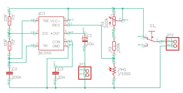
In this dark detector circuit, the 555 timer IC is in astable mode. The activation of the IC is controlled by photoresistor (LDR) and variable resistor (potentiometer). When the resistance of LDR increases and the potentiometer in minimum resistance the RESET pin (pin 4) will get voltage so the IC is activated. And then when the resistance of LDR decreases and the potentiometer is still in minimum resistance the RESET pin (pin 4) will not get voltage so the IC is not activated. Before explaining how to make the dark detector circuit I will share a little about the 555 timer IC.
555 timer IC was first designed and made by Hans R. Camenzin d in 1970. The name 555 is taken from three 5k ohms resistors contained in the IC. It is a highly stable IC that can produce accurate time delays and oscillations. The 555 timer has three operating modes, bistable, monostable and astable. In general, the 555 timer IC used is an 8-pin DIP (Dual Inline Package) IC timer.
The configuration of the 555 timer IC with 8 pins will be shown in this table below
| PIN | NAME | FUNCTION |
| 1 | GND | Ground reference voltage, low level (0 V) |
| 2 | TRIG | The OUT pin goes high and a timing interval starts when this input falls below 1/2 of CTRL voltage (which is typically 1/3 Vcc, CTRL being 2/3 Vcc by default if CTRL is left open). In other words, OUT is high as long as the trigger low. The output of the timer totally depends upon the amplitude of the external trigger voltage applied to this pin. |
| 3 | OUT | This output is driven to approximately 1.7 V below Vcc, or to GND. |
| 4 | RESET | A timing interval may be reset by driving this input to GND, but the timing does not begin again until RESET rises above approximately 0.7 volts. Overrides TRIG which overrides threshold. |
| 5 | CTRL | Provides “control” access to the internal voltage divider (by default, 2/3 Vcc). |
| 6 | THR | The timing (OUT high) interval ends when the voltage at the threshold is greater than that at CTRL (2/3 Vcc if CTRL is open). |
| 7 | DIS | Open collector output which may discharge a capacitor between intervals. In phase with output. |
| 8 | VCC | Positive supply voltage, which is usually between 3 and 15 V depending on the variation. |
Now after knowing about the 555 timer IC and it’s configuration. We will turn into how to make a dark detector circuit.
Step 1: Schematic and Board Design
Schematic and board designs can be created using Autodesk Eagle 9.5.1 software. We use this version or above, so later we can link the board to Autodesk Fusion 360 for the 3D board design
Schematic:
Board:
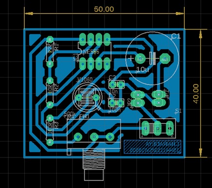
When dealing with PCB design, there are some things that we should pay attention to. The first is the diameter of the pad in the design, the diameter must be following what we need because if it is too small then the component legs will not be able to enter while if it is too large the results of the PCB will look bad. The second is the width of the wire, the size of the wire that is too thin will make it dissolve in the etching process of the PCB, so the results of the PCB fails.
Schematic and board can be downloaded at:
https://drive.google.com/open?id=1Jr-Ku8OvS9CHrGc3bDx36c9ALXtjwvfi
Then transformed the board design of the circuit into a 3D PCB display using Autodesk Fusion 360 software.

Step 2: Design Simulation
The schematic circuit can be simulated using Proteus software. The pictures below will show the simulation result.
Condition 1: Low light intensity (dark)

IC is activated and the output (speaker) turn on or make a sound
Condition 2: High light intensity (bright)

IC is deactivated and the output (speaker) turn off
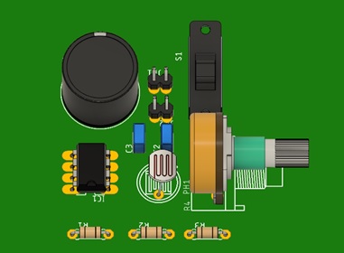
Step 3: Printing and Assembling The Dark Detector Circuit
The tools and materials needed to make this circuit are
Tool:
- solder
- drill
Material:
- 1 PCB board single side : 5cm x 4 cm
- 1 IC NE 555
- 1 LDR
- 3 Resistor: 10k, 22k, 100k
- 1 Potentiometer 1M
- 1 Electrolytic capacitor
- 1 Ceramic capacitor
- 1 Speaker: 8 ohm 0.4 Watt
- 1 Battery: 9 volt
- 2 Pin header: 1×2
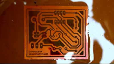
There are many ways to print PCB, the simple one is ironing. In this way, we iron the paper that contains the board design on the PCB board so that the design attached to the PCB board, where the copper covered will later become the PCB path.

After that, we will etch the PCB with ferric chloric (FeCl3) and water (H2O) solution. After the dissolution process is complete the PCB board is cleaned with water so that the PCB path can be seen
PCB is in dissolution process :
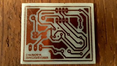
After dissolution process :
The next stage is the assembly, but before we have to perforate the pad components on the PCB by using a drill.
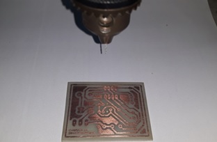
And finally, we can put components in place, components are bound using solder and lead.
PCB Dark Detector Results.

That’s all my article about the dark detector circuit. Thank you for reading.
Designed by Chairadeya (19/441153/SV/16505)